

The standard software for photonic chip design
Pioneering photonics design automation already since 1991, today PhoeniX Software has a global presence and is a trusted and well recognized partner for a large number of organizations. We enable easy and cost-effective realization of integrated photonics chips and systems, by means of our internally developed superior products and services. Our customers range from large OEM's to start-ups and include some of the worlds top universities and research institutes.As the leader in Photonic IC design solutions, we will continue to develop the market by anticipating market demand and customer needs. In combination with our strategic partnerships, this results in offering world class design flows and access to all relevant fabrication technologies for our customers.
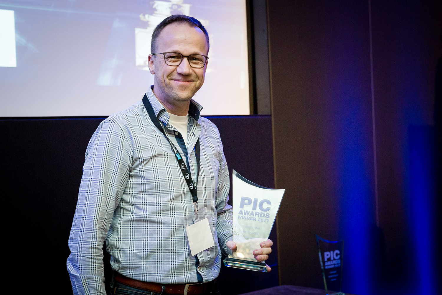
NOMINEES
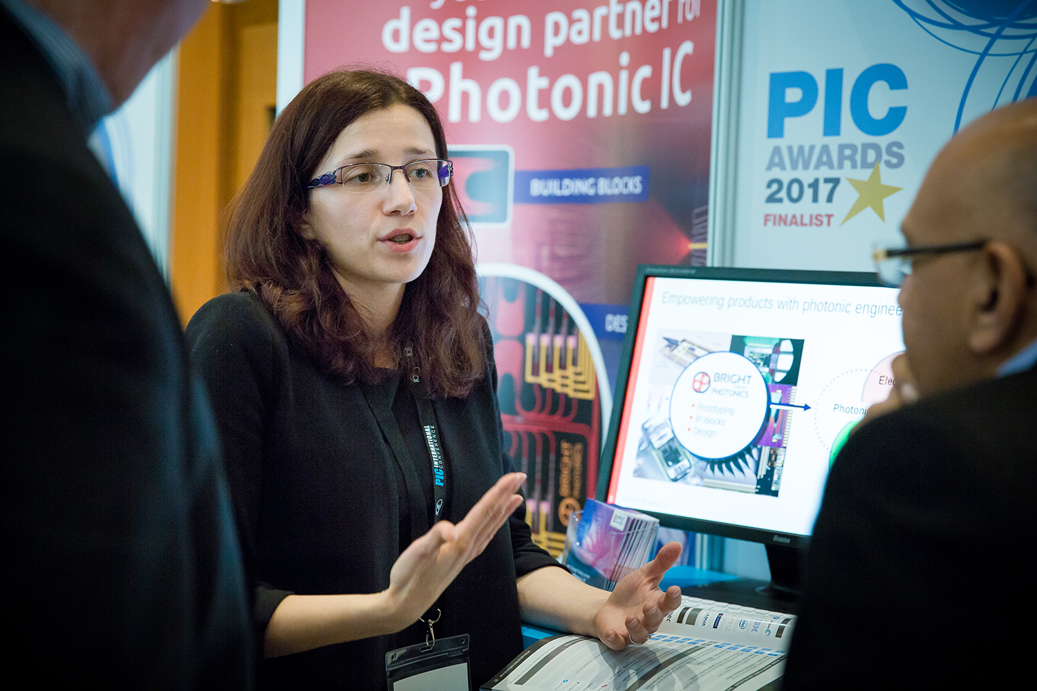
VLC Photonics, BRIGHT Photonics, Luceda Photonics, Kaiam Corporation

Lasers, optical components, modules and subsystems for the optical, industrial, and consumer laser markets
Oclaro is one of the largest providers of lasers and optical components, modules and subsystems for the optical communications, industrial, and consumer laser markets. Oclaro has enabled an almost complete on wafer test (OWT) of InP PICs. They can automatically identify known good die for assembly and map all key parameters at wafer level to maintain process control and integrity. Adding the OWT capability to Oclaros InP platform is a huge step towards the reduction of manufacturing costs for InP based PICs.
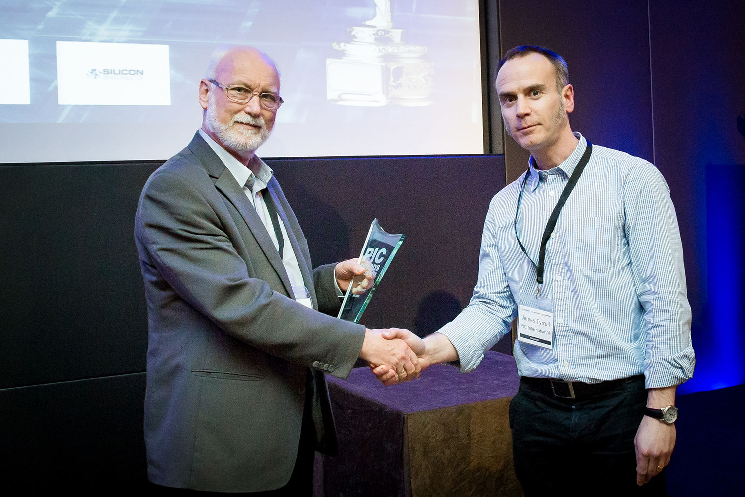
NOMINEES
Yelo Limited, Prof. Zeev Zalevsky

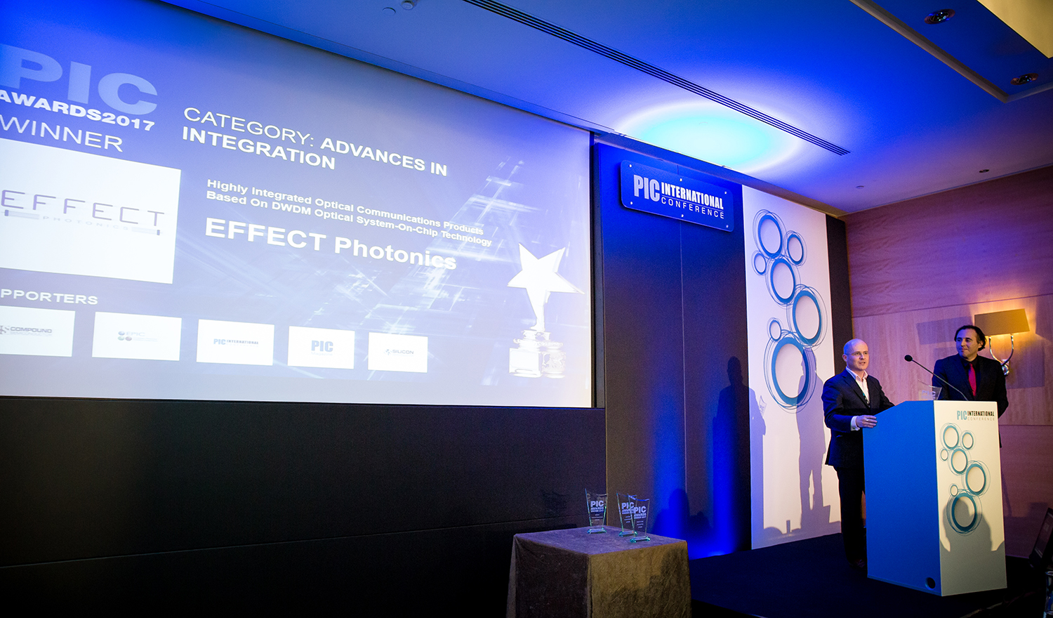
Highly integrated optical communications products based on DWDM optical System-on-Chip technology
EFFECT Photonics develops highly integrated optical communications products based on its DWDM optical System-on-Chip technology. The key enabling technology for cost effective DWDM systems is full monolithic integration of all photonic components within a single chip, also known as Photonic Integrated Circuits (PICs). This technology combined with EFFECT Photonics' low cost packaging capability, addresses the soaring demand for low cost DWDM solutions in high bandwidth connections between Datacenters (Inter-Datacenter), mobile cell towers for Fronthaul, Backhaul, and Passive Optical Networking (PON) applications such as NGPON2.
NOMINEES
Di Liang, Hewlett Packard, TOPTICA Photonics, IBM, Acacia, Skorpios, Infinera, Mellanox, Colorchip, IHP, Sicoya

Production services for Indium Phosphide (InP) based photonic components
SMART Photonics, is a Pure Play Foundry offering production services for Indium Phosphide (InP) based photonic components. They offer the complete creation process from first Epitaxial growth, high resolution lithography, re-growth, wafer processing, metallization, polishing of wafers up to the coating of the chip facets. SMART Photonics has further developed its generic integration technology for integration of InP basedphotonic components. For this new technology, free access to the SMART Photonics design manual is offered to customers to design their own PICs. Designs can be easily, and cost effectively, tested in the SMART Photonics MPW-runs.
NOMINEES
Physik Instrumente GmbH, Luxtera, ficonTEC, LioniX International, Cisco

Using silicon photonics integration to address data center demands
Using Silicon Photonics Integration to Address Data Centre Demands
IntroductionSince the Renaissance, our world has been shaped by technology, and every age has its transformative phenomenon that burns across society reshaping human life and culture: crop rotation fuelling the agricultural revolution, the steam engine freeing up human and animal muscle power, steel allowing railroads and industrialisation which in turn fuelled Europe's dominance of the world, to the transistor and the integrated circuit which has brought us the modern age. Clearly the dominating technology of our day is the internet and the communication infrastructure that has brought the world both together and fractured it at the same time.
Google, Facebook, Instagram, Amazon don't just supply information, but are fundamentally changing the way we interact and see each other. Boundaries between countries dissolve, while similar groups of geographically diverse individuals band up in international organisations. Information is key, and mining big data in the massive supercomputers determines elections and corporate valuations. The underlying technology is the massive data centre. Typically 250,000 square feet or more in size, and placed close to sources of cheap power, these immense supercomputers consume about 5% of the world's electricity. Within these giant warehouses, there are 100,000s of servers all connected through switches and fibre-optics. A typical Google search spreads through more than 1000 servers through the fibre-optic backbone, the servers comparing information and prioritising a list based on the searcher's history and assumed intent. At the same time, customized adverts, targeted to the individual is what generates the revenue. The more powerful the data centre and the more it knows about you, the more likely you are to buy the recommended product.
Moore's Law has been at work for decades now, improving the microprocessors and the switches that connect them to power the data centre. Optics and lasers, however, do not follow the same scaling laws. What is now the bottleneck is the fibre-optic network that connects the servers together. Information may trickle in and out of the data centre, with the consumer searching a word or a phrase, and targeted information returning, while at the same time a tsunami of data is passing through thousands of servers within the data centre to consolidate and customise the information based on everything everyone knows. The fibre-optic network within the data centre is what's funnelling the inter-server tsunamis.
This fundamental issue is that the switching and processing of data follow Moore's Law while the optical connection that transports data does not. This is the major impediment to the further growth of the data centre. (Bechtolsheim, 2012) As a comparison, consider that in the year 2000, a network switch in the data centre cost $4000 and carried eight lanes of traffic at 2.5Gb/s. The cost of the optical transceivers for 2.5Gb/s for short distance interconnect multi-mode was $50 each. So the total cost of the switch to the optics was about 10:1. Fast forward to today, where the switch still costs $4000, but thanks to Moore's law now carries 32 ports of 100Gb/s. The optics required for this high data rate, over the longer distance of single mode fibre, costs about $1000 each. So the numbers become obscenely reversed, where $32,000 of optics is required to connect a $4000 switch.
This is clearly an untenable situation. Data centres cannot grow unless the cost of the optics drops dramatically. Current solutions for optics generally use standard approaches using discrete components such as thin film filters and glass lenses, all manually assembled in order to obtain the necessary alignment tolerances required for optics. The market for transceivers used in this space is estimated to be huge at about $1B and growing at between 35%-40% per year (LightCounting, 2016). Clearly a solution that can provide this functionality at a lower cost can be a breakthrough for the industry.
Recently there has been tremendous interest in silicon photonics where integrated circuit technology is used to make the optics for the transceivers. This relies on other properties of silicon to generate, modulate, and combine different wavelengths of light. Unfortunately, though silicon is an outstanding material for switching electrical current, it is woefully inadequate for these optical functions. Thus using the integrated circuit infrastructure to make low cost multi-wavelength optical transceivers has been mostly a dream undermined by the physics of the material itself. Though some silicon photonics has been deployed using parallel fibres, the technology has been unable to address the core market that uses multiple wavelengths over the same fibre (Dobbelaere, 2016). For example Intel, which has spent hundreds of millions of dollars on silicon photonics making numerous announcements over the last decade (Christy, 2015) has only recently brought out a product (Takahashi, 2016), and that once again uses the much less desirable multiple fibre format.
Technology Background In the data centre, pluggable transceivers are used to convert the electronics signals from the switch or router into optical signals that travel down optical fibres. Generally multiple signals travel down a single fibre to increase the bandwidth using wavelength multiplexing. For example, a 100Gb/s signal travelling down a single fibre is actually composed of four separate 25Gb/s signals, each one coded to a different wavelength of light. Thus to make a multi-wavelength optical transceiver one requires four separate sources at the transmit and four separate detectors at the receive end with wavelength multiplexing and demultiplexing of the signals integrated in the module. Thus for the transmitter one needs multiple laser sources, multiple ways of modulating the light from these lasers, a method of combining the multiple wavelengths of light together, and electronics to drive and control the transmitter. On the receiver side, one requires a method of demultiplexing the multiple wavelengths of light, detecting the light, then amplifying and regenerating clean electronic signals.
Unfortunately silicon is not ideal for all these functions. Of course one can do the signal processing, the drivers, the amplifiers and signal regeneration in the silicon using standard components. And these blocks have been improving dramatically according to Moore's law. One can even fabricate relatively good detectors and modulators using germanium containing processes to make detectors and silicon-on-insulator waveguides with pn junctions for modulators. However, the lasers are extremely difficult, as to generate light one needs a direct-gap semiconductor. Similarly dispersive components such as wavelength multiplexers and demultiplexers are challenging as the high temperature dependence of silicon's refractive index makes them unstable, and wavelength control is further compromised by the very high index contrast between silicon and silicon dioxide. The latter results in extremely poor yields. Ideally one should use indium phosphide (InP) for the laser sources and glass waveguides for the latter. InP lasers are robust, efficient and mature, and can be made at very low cost. Similarly, glass waveguides are beautifully transparent and can easily be formed using lithographic processes into stable and high yield mux/demux structures. These planar lightwave circuits (PLCs) with glass waveguides are already used in high density long haul communications to multiplex and demultiplex up to 96 channels.
So far practical silicon photonics has been missing the multiplexer/demultiplexer and only a single laser has been used due to the complexity of the packaging. Without the ability to combine and split wavelengths, these silicon photonics transceivers have needed multiple fibres and transmit the four signals with only one channel per fibre (Dobbelaere, 2016). Needing four separate fibres makes the fibre plants in the data centre much more expensive and adds complex array connectors at all the patch panels. The problem becomes more acute as systems in the future require 8 channels to further increase speed.
Kaiam InnovationIn order to compensate for the deficiency in silicon to generate and multiplex light we developed a SiP (System-In-Package) structure where glass waveguides together with laser diodes that are MEMS-coupled are simply mounted on a silicon photonics chip. The silicon photonics hybrid chip assembly is a commercial IC meant for multiple-fibre applications. In fact, the silicon photonics chip consists of two chips that are combined using a copper pillar process. The larger chip below contains silicon modulators and detectors while the top chip contains the drivers, amplifiers and signal regenerators (CDRs- clock-data-recovery). The PLC is the glass waveguide chip fabricated by Kaiam which contains the multiplexer and demultiplexer elements. Four lasers, each at a different wavelength are attached to the PLC using Kaiam proprietary MEMS alignment. The light enters and exits the assembly through single mode fibres epoxied to the glass PLC. Finally the optical path between the PLC and the commercial silicon photonics chip is obtained by angle polishing the waveguide chip that deflects the optical beam down to a set of grating couplers integrated on the silicon photonics chip.
SiP consisting of a commercial silicon photonics chip with the Kaiam glass waveguide PLC and lasers. Compensating for silicon's deficiencies, this is the first multi-wavelength silicon photonics transceiver.
There are in fact two microcontrollers in the complete transceiver. The silicon photonics IC contains a controller that adjusts the bias and voltage on the modulators, monitors the regenerator thresholds and compensation and controls the various internal settings of the transceiver. In addition, the module electronics contains four laser drivers and associated control loops, all programmed by a second microcontroller on the board. The software has to compensate and adjust for temperature, input power levels, and other variables and set and adjust various status and error flags that are communicated using an I2C interface. To calibrate the modules, custom testers have been built that monitor the bit-error-rate on the receiver and the transmit eye under various conditions. The calibration data is stored in the non-volatile memory. The figure shows the transmit eyes at 700C, showing clear open eyes at 25Gb/s.
These fully functional transceivers are now being sampled and qualified by major tier 1 data centre companies. We believe this architecture more than halves the cost of the transceiver and is far easier to fabricate than alternative architectures.
This is clearly a very exciting time for the company as we prepare to ramp this new System-in-Package transceiver architecture.
SummaryOur society is shaped today by data centre architectures that control the flow of information. The bottleneck in data centres is not so much the servers and the switches, but the communication network that connects them together in order to allow massive parallel processes. The issue is that fibre optic transceivers do not obey Moore's law and have not scaled as fast as the electronics. Kaiam is addressing this bottleneck by complementing the silicon with glass waveguides and InP lasers. This allows silicon photonics to address the demanding data centre applications. This packaging platform was used to build complete transceivers that are being scaled today.
Works CitedBechtolsheim, A. (2012). Moore's Law and Networking. NANOG55, North American Network Operators Group. Vancouver, British Columbia, Canada: nanog.org.Christy, P. (2015, 2 17). Retrieved from 451 research: 451research.comDobbelaere, P. D. (2016). Deployment of siliucon photonics technology in data communication applications. International Conference on Optical MEMS and Nanophotonics (OMN). Singapore.LLC, L. (2016). High-Speed Data Center Optical Interconnects. Eugene, OR: lightcounting.org.Takahashi, D. (2016, 8 17). Intel debuts silicon photonics module for lightning-fast connectivity in data centers. Retrieved from Venture Beat: venturebeat.com
NOMINEES
LiGenTec, Lumentum, Oclaro

Leading contributions to the development of an InP PIC ecosystem in Europe
Meint K. Smit invented the Arrayed Waveguide Grating, for which he received a LEOS Technical Achievement award in 1997. In 2000 he became leader of the Photonic Integration group at the COBRA Research Institute of Eindhoven University of Technology. His current research interests are in InP-based Photonic Integration, including integration of InP circuitry on Silicon.
"Weve analysed the success of microelectronics. Now were putting those lessons learned to work for integrated photonics" says Professor Meint Smit, Eindhoven University of Technology.
The development of silicon based microelectronics means today it costs only a few cents to design and develop per square millimetre of chip, as the technology is mature and highly standardized. In addition, its development costs are low because we have sophisticated software for the fast and accurate design of the chips. Teams at Eindhoven University of Technology, led by Professor Meint Smit, want the same for photonic devices. And now that tipping point has been reached.
"Around the start of this new century, we were all asking ourselves: when is photonics integration really going to take off in the same way as silicon micro-electronics?" explains Smit. "After all, in 1980 I had started saying it would kick start in the 1990. Ten years later, the tipping point had moved to the start of the new millennium. By that time, some critics started to say that the promise of photonics integration would always remain in the future."
Understanding the success of microelectronics"In Eindhoven, we looked at the world of microelectronics and discovered that things were arranged in a very different way. Up until the 1980s you had a lot of different technologies being used. There were a whole range of transistor types and countless variations between them. But in the 1980s things started converging and you started to see the development of generic processes."
"Designs start to use the same basic building blocks of transistors, resistors and capacitors. Even some of todays most complicated processors, with over 1 billion transistors, have less than 10 different components. So you are using the same set of building blocks to create all kinds of things."
"We asked ourselves, how can this be applied to photonics? If you look to light, it has an amplitude, a phase and a polarisation. So if you make a component for manipulating phase, another for changing polarisation, and one for altering phase, you could achieve a lot of things. Then you simply need a waveguide to connect them."
"So we started developing a process with an optical amplifier for the amplitude, a phase modulator to change the phase, and a polarization converter."
"There is a big advantage if everyone uses the same generic process. You can combine a lot of different designs on one chip. In a recent successful test case, we had 20 different designs on one wafer."
Theres always more than one run"The challenge in this business of integrated photonics has been the cost of making a chip prototype. If you develop a chip it always takes 2-3 runs before you get it right, because the chip never performs exactly as you expect."
"Traditionally, one process run currently costs at least 200,000, if you do it on your own. So this is a huge barrier for small companies. But if 20 users can share the same wafer, then the costs drop to 10,000 each and thats within the scope of many startups. You get 8 identical cells back from the foundry which you can test and measure. You can then iterate the design, so that the next run gives even better results."
Open Collaboration is key to maintaining Europes LeadEindhoven Technical University (TU/e) also drives and actively contributes to the International JePPix platform. This is an open collaboration between over 240 members, designed to connect researchers, PIC designers, and generic foundries to dramatically cut costs and speed up the time to market. TU/e have also set up Smart Photonics, the only foundry in the world dedicated to the production of low volume Indium Phosphide chips.
"The role of Jeppix is to act as an independent broker between designers and foundrys. We announce a production schedule, collect the designs and produce one big mask. That goes to the foundry that produces the wafers, cuts them up and sends the result back to the various designers. So this is the way TU/e has introduced generic photonics manufacture into Europe."
The race is on"Clearly, others have recognised were on to something. In October 2014, US President Obama reserved US$ 220 million to set up something similar in the United States. Several leading universities and technology companies there are bidding in the tender to create the "Integrated Photonics Institute for Manufacturing Innovation". Everyone in the industry is waiting to see which city gets to host the institute, because it will mean the creation of many local jobs in the USA for whoever wins."
"It turns out that the generic integration process is quite complex, so being able to master this gives us a head start. But weve reached a very important tipping point. And when we look at the world of semiconductors, no-one thought such generic processes could ever drive very fast 60 GHz radio frequency circuits. Personally, I think if you are willing to invest enough money in a single technology, then it will surpass the rest."
Indium Phosphide Wins on Price"Now, lets suppose your chip works and youre happy with its performance. Then scaling up to produce 100,000 pieces is no problem. You can order them immediately knowing that the specs will remain constant. This part can be done using a more traditional process. A large Photonics foundry like Oclaro can manufacture 10,000 wafers a year."
"The other point is the chip cost. We are actually cheaper. Of course, silicon photonics can make their chips cheaper if you buy a million, but few small companies want a million. They want to start with a few hundred or a few thousand. And if you want a few hundred from a silicon foundry then the entry/set-up costs are very much higher than in photonics. So if you look at the functionality per Euro, Indium Phosphide wins and we are very competitive in the lower volumes."
"The next step, and we have the first products lined up for that, is to do the whole thing again but then not on a substrate of Indium Phosphide, but on Silicon. But then we will add a very thin layer of Indium Phosphide."
Riding the Seven League boots of Silicon"The holy grail of this industry is to put lasers onto a piece of Silicon. Silicon itself is not suitable for this you cant generate light directly, whereas with Indium you can generate light directly on the substrate. Weve validated methods to build a photonic component on an Indium Phosphide layer and then connect it to a Silicon layer underneath. We are in the process of launching the first working devices."
"We think that Indium Phosphide will champion by using the "seven league boots of silicon" and we believe our generic approach will scale faster."
NOMINEES
Arjen Bakker, Hans van den Vlekkert & Rene Heideman